You are here
Profilometers using Low Coherence Interferometry used by NASA to measures thickness

Using a fiber-based optical profilometer NASA measures the thickness of liquid nitrogen in cryogenic chambers at its Propulsion Systems lab because these profilometers use fiber-based probes which can withstands the extreme environment, can be located hundreds of meters away from the interferometer and fit in the tight chamber which standard full-field profilometers with a human operator could not. The signal quality stays constant over the distance.
White light interferometry has long been used in metrology fields to obtain micron-scale measurements and imaging of surface characteristics, cross-section imaging, and material thickness measurements. Still, a number of applications require particular versatility from their inspection system, beyond what is possible with a full-field profilometer. Certain applications call for measurements of long profiles (not possible with full-field), others need to measure translucent material thicknesses on moving surfaces like webs, others still require mapping of larger surfaces, without the need for tiling. Also, some surfaces are particularly difficult or impossible to inspect with full-field interferometers: the insides of small diameter tubes, the outsides of cylinders, as well as concave or convex spherical surfaces. Further complications are posed by surface inspection in environments involving radioactivity, extreme heat or cryogenic temperatures. To answer these challenges, the Canadian company Novacam has developed a fiber-based optical interferometer system and a wide selection of non-contact probes to suit laboratory or online installations. Fiberbased probes can be deployed far from the interferometer enclosure. They can be mounted onto a variety of positioning systems, facilitating integration into production lines and making many hard-to-reach surfaces accessible for imaging. The system offers the ability to scan long profiles and to map larger contiguous surfaces. Moreover, multiple probes can be connected to an interferometer with the help of an optical switch, thus lowering the cost per probe.
Principles of Optical Interferometry
A low coherence interferometer uses broadband light (1,300 nm wavelength). Light reflected from the sample creates interference patterns that determine the distance between the probe tip and the sample, with a precision better than 1 µm. Unlike full field interferometers or line sensors, which scan a small surface or a line at a time, a fiber-based probe acquires one point at a time and is typically displaced over the surface with a scanning mechanism.
What Kind of Surfaces?
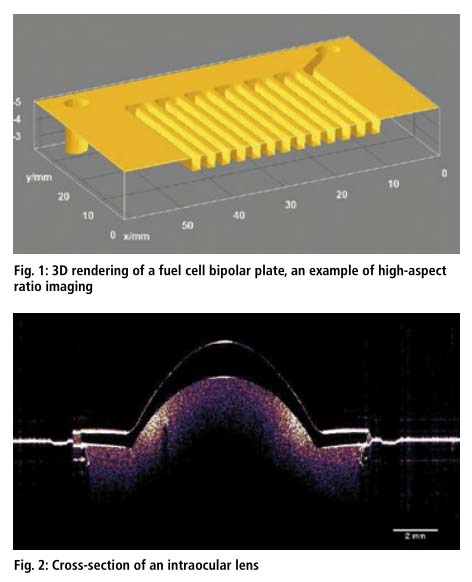
Any surface, solid or liquid, can be scanned, mapped and characterized to sub-micron resolution. This includes surfaces with steep slopes and high-aspect ratio features like channels on fuel cell bipolar plates (fig. 1), grooves on CMP pads for polishing wafers, or cooling holes in aerospace blades. Such surfaces present a challenge to competing technologies. Triangulation sensors, for example, have trouble imaging high-aspect ratio surfaces. Neither triangulation nor color confocal systems can match the sensitivity or ruggedness of low coherence interferometry when it comes to high-aspect feature imaging. Because the Novacam profilometer emits and picks up light with a single probe, it is able to measure and image high-aspect ratio surfaces.
Measurements Delivered
The probe scans the surface from a standoff distance of 1 to 150 mm, at a rate of 1 to 30 kHz depending on the model. Thousands of light interference measurements create a 3D image of the surface, facilitating defect detection. Given the point cloud data, application software calculates surface characteristic parameters, including surface roughness and waviness. For surface defects caused by wear or abrasion application software determines volume loss.
When used in cross-sectional mode, the interferometer obtains thickness measurements and cross-section imaging of translucent coatings or films whose optical thickness ranges from 10 µm to 8 mm. Materials differ in their translucence and light refraction characteristics, permitting the interferometer to detect reflections from the entry and exit of each material layer. Whether the scanned films are single layer or multilayer, thickness measurements are thus obtained simultaneously. Inspecting products such as an intraocular optical lens or a contact lens becomes intuitive: the interferometer provides a cross-sectional image (fig. 2) and calculates material thickness at any point desired. It can show volume density maps and 3D isosurfaces. The results can be analyzed for cracks, bubbles and other defects, and lens curvatures can be calculated.
Hard-to-reach Surfaces
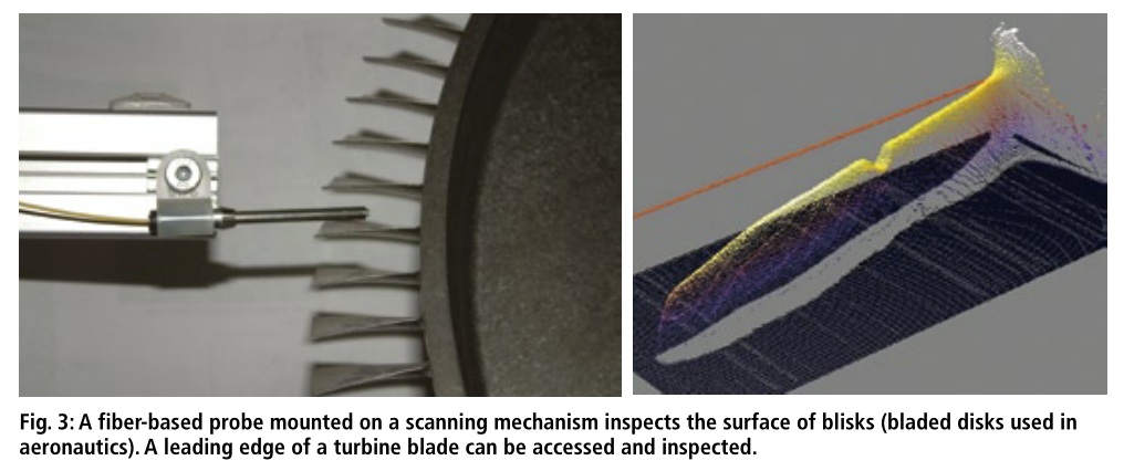
Traditionally, hard-to-reach surfaces, such as interiors of aeronautics components, have been measured by taking a mold of the interior space and bringing this replica under a full field profilometer. In contrast, small-diameter fiber-based probes inspect surfaces inside tubes and other tight spaces directly. Probe diameters range from 0.9 to 5 mm. The probes are mounted on either a combination of two or three linear or rotational axes, or on a CNC machine or a coordinate measuring machine. For example, a scanning arm inserts a side-facing probe between closely spaced blades of an aerospace engine blisk (fig. 3). Leading edges of turbine blades can be accessed and inspected similarly. A scanning probe can inspect the interior of a diesel fuel injector, or the cylindrical cavity of an engine block, or of a gun barrel. Inspecting smaller tubes, with diameters as small as 2â€"10 mm, is made possible with flexible two meter long side-looking (90°) rotational probes with pullback.
Probes in Action in Process or lab
Since fiber-based probes can be located hundreds of meters away from the interferometer enclosure without signal degradation, a variety of operating environments become possible. For one, probes are readily placed for in-line measurement. When mounted onto linear scanning stages, they are able to scan across fast-moving production webs, delivering long profile or thickness measurement in real time. Multiplexing of probes which are connected to one interferometer offers additional potential value. 2D Galvo probes (with light-deflecting mirrors attached on a galvanometer) are effective for scanning smaller surfaces (less than 15 x 15 mm) or volumes. Combined with a linear stage, a band of up to 1.5 cm wide can be acquired. These are ideal for applications such as inspecting electronic packaging and MEMS or optical lenses. The rugged probes are also able to operate in hostile environments, including radioactive chambers, very hot environments (in proximity to molten metal) and cryogenic environments. Thus, even the simulation of outer space condition at NASA is made possible.
Contact:
Novacam Technologies Inc
277 Lakeshore Road, Suite 04
Pointe Claire, QC.
H9S 4L2
http://www.novacam.com
tel: (514) 694-4002
fax: (514) 630-6420
e-mail: info@novacam.com
| Attachment | Size |
|---|---|
| 504.79 KB |
- profilometer's blog
- Log in or register to post comments
- 7357 reads
Recent comments