
Sheng Xu, University of California, San Diego
1. Introduction
Conventional microfabrication techniques are 2D, such as photolithography and electron beam lithography, which can generate patterns on planar wafers and thin films. However, our world is 3D. There is an unmet need for synthesizing and assembling functional materials and devices in 3D for potentially better properties and performance. Existing approaches for 3D microfabrication, including direct laser writing [1], interference lithography [2], glancing angle deposition [3], inkjet printing [4], on-wire lithography [5], using templates [6], and self assembly [7], have proven to be effective and valuable in various aspects, but they either cannot be scaled up, or are limited to certain classes of materials. Stress has emerged as a powerful means that provides unprecedented capabilities in fabricating 3D microstructures based on a wide range of materials on large scale. In this discussion thread, I am highlighting from the literature a few representative examples of stress guided 3D microfabrication, to illustrate their unique features and capability to complement conventional microfabrication methods.
2. Residual stress driven bending and coiling
Residual stress in the thin films, when unconstrained, will bend 2D materials and devices into tubes and helices. The residual stress can be from lattice mismatch during the epitaxial growth process, difference in thermal expansion coefficient, or the nonuniform/anisotropic modulus distribution in the materials after post processing.
2.1 By growth/deposition
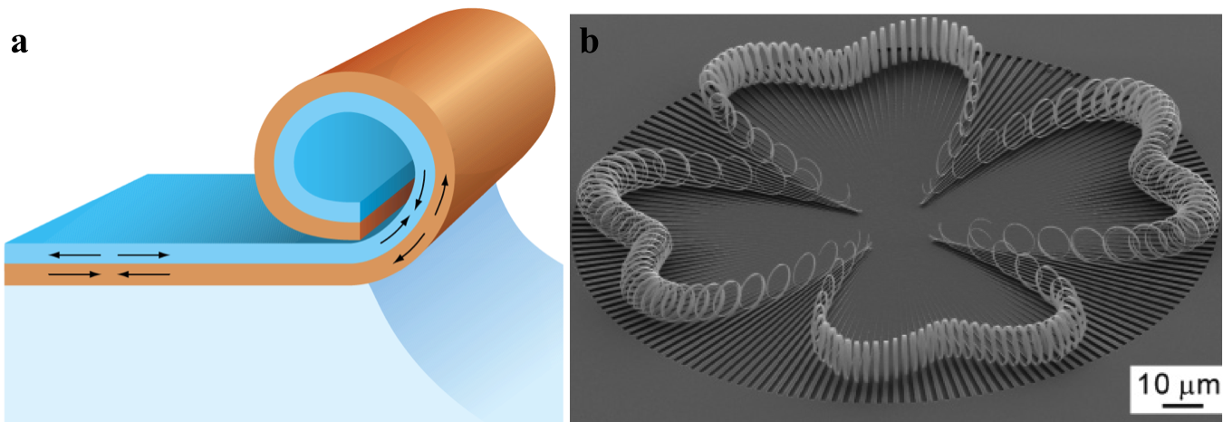
Due to the finite differences in lattice constants of crystalline semiconductor materials, there will be residual stress in the as grown crystalline thin films on top of the epitaxial substrate (Figure 1a) [8,9]. Depending on their relevant sizes, the stress can be tensile/compressive, if the lattice constant is smaller/larger in as-grown thin films than in the underlying epitaxial substrates. When the stressed thin film is detached from the underlying substrate, the residual stress will drive the thin film to curl up into tubes or helices (Figure 1b). It applies to crystalline semiconductors or even multilayers of materials as a functional device [10,11], but it can only generate limited geometries, such as tubes and helices, and therefore have limited examples of device integration.
Figure 1. (a) Schematic illustration of the residual stress induced bending. In this case, the top layer has tensile stress and the bottom layer has compressive stress. When they are unleashed, the top layer contracts and the bottom expands, leading to an upward curl; (b) SEM image of 3D structures formed from a bilayer of p-type crystalline Si coated by amorphous Cr [9,12].
2.2 By post processing
Post processing, in combination with lithography or printing, can generate nonuniform/anisotropic modulus distribution, and therefore induce residual stress in the material when the temperature is changed, the materials is swelled by a solvent, or the solvent is evaporated.
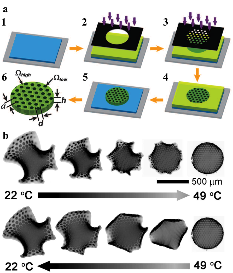
For example, with photolithography, the degrees of crosslinking in polymer precursors are different across the surface (Figure 2). Areas with high degree of crosslinking will be more rigid and have a high thermal expansion coefficient than those with low degrees of crosslinking. When the surrounding temperature is changed, residual stress is induced at the hard/soft boundaries. The residual stress will bend the material, and by strategically controlling the distribution of these hard and soft regions, different geometries of materials can be realized [13].
Figure 2. (a) Schematic illustration of the fabrication process for embedded nonuniform rigidity. (1) On a silicon wafer coated with a sacrificial layer, (2) the photosensitive polymer film is cast and exposed to a small dose of UV light through the first photomask and subsequently (3) a large dose through the second photomask. (4) The patterned film is (5) developed to remove uncross-linked material and (6) immersed in aqueous solution to release it from the substrate and induce swelling, where Ω indicates areal expansion ratio. (b) Reversible thermal actuation of patterned sheet but through different pathways [13].
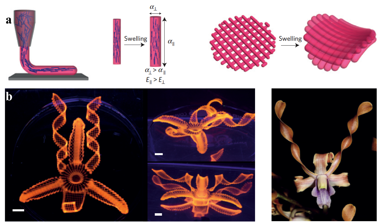
In another example, a soft polymer matrix is embedded with cellulose fibers. When they are squeezed out of a nozzle, i.e. when being printed on a substrate, these fibers align by flow field driven self-assembly [14]. The alignment of the fibers in the polymer matrix results in an anisotropic modulus of the printed polymers. Therefore, when immersed in solvent, the printed polymers in predefined layouts and configurations will swell anisotropically that leads to curved surfaces (Figure 3).
Figure 3. (a) Schematics of the flow-field induced alignment of cellulose fibers during direct ink writing and subsequent effects on anisotropic stiffness E and swelling strain alpha, which result in anisotropic deformation behavior. (b) A biomimetic-swollen structure of a flower (left panel) demonstrating a range of morphologies inspired by a native orchid (right panel) (scale bars 5 mm) [14].
This approach can generate a wide class of structures and configurations, but it is limited to amorphous or composite polycrystalline materials, which are less useful in high performance electronic devices.
3. Compressive buckling on prestrained elastomeric substrates
It exploits compressive force from the prestrained elastomeric substrate to fabricate 3D microstructures. Specifically, the 2D precursor materials are bonded on a prestrained elastomeric substrate. When the prestrain is released, the compressive stress will force the unbonded material into the third dimension. This process is reversible. When the substrate is stretched, the 3D structures can collapse and become 2D again. The precursor material can be uniformly or selectively bonded on the prestrained elastomer, which leads to different geometrical and functional outcomes.
3.1 With uniform bonding
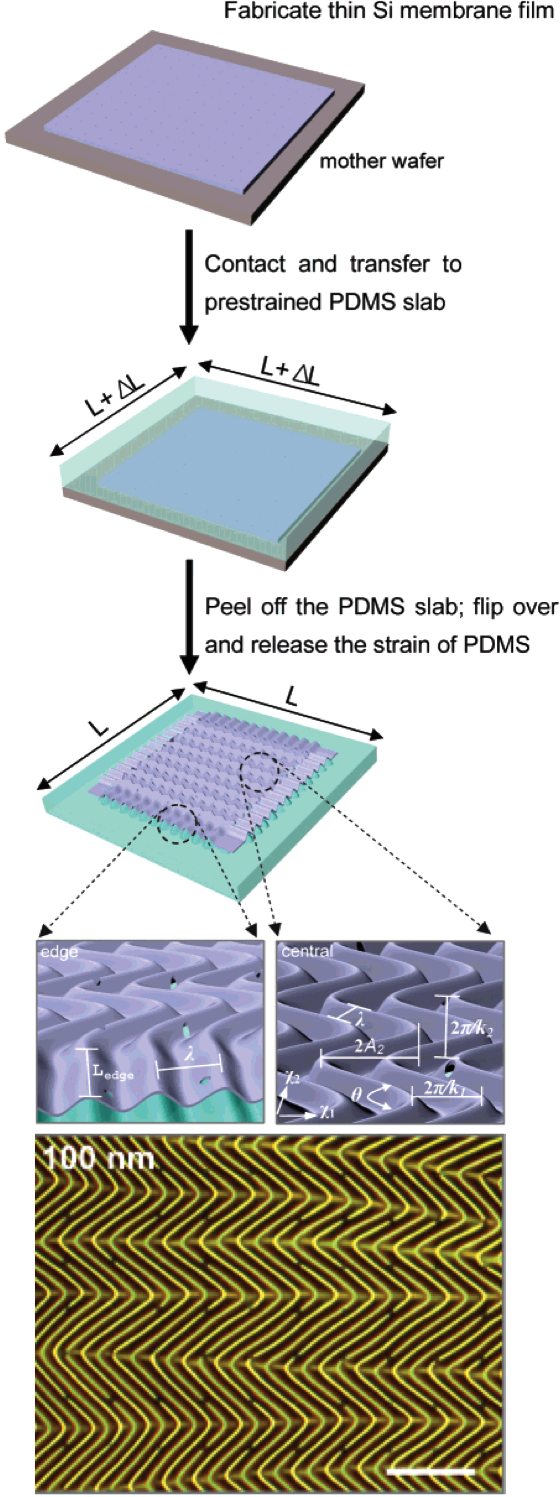
Uniform bonding requires the precursor materials to remain inintimate contact with the elastomeric substrate without delamination throughout the entire process. The resulting wavy geometry, such as the wave period and amplitude, depends on a combination of factors, including the prestrain level, moduli and thicknesses of the substrate and the precursors. This strategy applies to both uniaxially [15] and biaxially [16]prestrained substrates (Figure 4). Demonstrated examples of this strategy include Si membrane [15,16], Si nanowires [17,18], ZnO nanoribbons [19], and carbon nanotubes [20,21]. This strategy works well when the prestrain level is relatively small, generally <10%, beyond which the precursors start to delaminate from the substrate or fracture.
Figure 4. Schematic illustration of steps for fabricating two-dimensional, “wavy” semiconductor nanomembranes on a prestrained elastomeric substrate. At the bottom is an optical micrograph of 2D wavy structures in silicon nanomembranes [16].
3.2 With selective bonding
To enable the structure to tolerate large magnitudes of prestrain level, a method called selective bonding can be used. In this case, the precursor is bonded to the prestrained substrate via nonreversible covalent bond through a designed set of locations, and the rest of the precursor is free standing (or bonded by weak van der Waals forces) on the substrate (Figure 5a) [22,23]. This reduces the strain localization at the bonded regions, and allows the application of a much larger prestrain level in the substrate, as supposed to the case of uniform bonding. The period of the buckled structure is determined by the pitch of the selective bonding locations, and the amplitude is controlled by the prestrain level. In addition, it gives us a degree of freedom to design the free standing region of the precursor, such as 2D layout (Figure 5b) [24,25], thickness [26], number of layers [27], so that they can lead to different configurations and functions.
Figure 5. SEM images of (a) an array of buckled Si membranes from linear 2D layout [22] and (b) an array of double layered helices from serpentine 2D layout [24]. Both cases are selective bonding.
This approach applies to general classes of materials including metals, polymers, and even device grade single crystalline silicon, as long as they are compatible with standard 2D microfabrication. This process is highly parallel, since all precursors can buckle simultaneously in one batch. The precursors have to be thin so that peak strain in the precursors is small to avoid any fracture.
4. Discussion
Stress has demonstrated great potential for fabricating advanced 3D microstructures, with features that are complementary to existing approaches. It allows integration of a variety of materials, including high performance single crystalline semiconductors, in a parallel, high throughput fashion. However, the demonstrated structures and functions are currently still limited. Further advancement in this direction will follow from fabricating any arbitrary structures by reverse engineering of the strain magnitude and distribution, 2D precursor layout, to probably strategic sequential bending/buckling of the precursors. With more structures available as building blocks, new devices and functionalities will naturally ensue.
5. References
1. Kawata, S., Sun, H. B., Tanaka, T., Takada, K., Finer features for functional microdevices - Micromachines can be created with higher resolution using two-photon absorption., Nature 412, 697-698 2001
2. Campbell, M., Sharp, D. N., Harrison, M. T., Denning, R. G., Turberfield, A. J., 1Fabrication of photonic crystals for the visible spectrum by holographic lithography, Nature 404, 53-56 2000
3. Robbie, K., Brett, M. J., Sculptured thin films and glancing angle deposition: Growth mechanics and applications, Journal of Vacuum Science & Technology a-Vacuum Surfaces and Films 15, 1460-1465 1997
4. Esposito, M., Tasco, V., Todisco, F., Cuscunà, M., Benedetti, A., Sanvitto, D., Passaseo, A., Triple-helical nanowires by tomographic rotatory growth for chiral photonics, Nature Communications 6, 2015
5. Luo, Z., Jiang, Y., Myers, B. D., Isheim, D., Wu, J., Zimmerman, J. F., Wang, Z., Li, Q., Wang, Y., Chen, X., Dravid, V. P., Seidman, D. N., Tian, B., Atomic gold–enabled three-dimensional lithography for silicon mesostructures, Science 348, 1451-1455 2015
6. Gao, W., Feng, X., Pei, A., Kane, C. R., Tam, R., Hennessy, C., Wang, J., Bioinspired Helical Microswimmers Based on Vascular Plants, Nano Letters 14, 305-310 2013
7. Tavakkoli K. G., A., Gotrik, K. W., Hannon, A. F., Alexander-Katz, A., Ross, C. A., Berggren, K. K., Templating Three-Dimensional Self-Assembled Structures in Bilayer Block Copolymer Films, Science 336, 1294-1298 2012
8. Schmidt, O. G., Eberl, K., Nanotechnology - Thin solid films roll up into nanotubes, Nature 410, 168-168 2001
9. Cho, A., Nanotechnology - Pretty as you please, curling films turn themselves into nanodevices, Science 313, 164-165 2006
10. Dastjerdi, M. H. T., Djavid, M., Mi, Z., An electrically injected rolled-up semiconductor tube laser, Applied Physics Letters 106, 021114 2015
11. Yu, X., Huang, W., Li, M., Comberiate, T. M., Gong, S., Schutt-Aine, J. E., Li, X., Ultra-Small, High-Frequency, and Substrate-Immune Microtube Inductors Transformed from 2D to 3D, Scientific Reports 5, 9661 2015
12. Zhang, L., Ruh, E., Grützmacher, D., Dong, Bell, D. J., Nelson, B. J., Schönenberger, C., Anomalous Coiling of SiGe/Si and SiGe/Si/Cr Helical Nanobelts, Nano Letters 6, 1311-1317 2006
13. Kim, J., Hanna, J. A., Byun, M., Santangelo, C. D., Hayward, R. C., Designing Responsive Buckled Surfaces by Halftone Gel Lithography, Science 335, 1201-1205 2012
14. Sydney Gladman, A., Matsumoto, E. A., Nuzzo, R. G., Mahadevan, L., Lewis, J. A., Biomimetic 4D printing, Nat Mater 15, 413-418 2016
15. Jiang, H., Khang, D.-Y., Song, J., Sun, Y., Huang, Y., Rogers, J. A., Finite deformation mechanics in buckled thin films on compliant supports, Proceedings of the National Academy of Sciences 104, 15607-15612 2007
16. Choi, W. M., Song, J. Z., Khang, D. Y., Jiang, H. Q., Huang, Y. Y., Rogers, J. A., Biaxially stretchable "Wavy" silicon nanomembranes, Nano Letters 7, 1655-1663 2007
17. Xu, F., Lu, W., Zhu, Y., Controlled 3D Buckling of Silicon Nanowires for Stretchable Electronics, ACS Nano 5, 672-678 2011
18. Ryu, S. Y., Xiao, J., Park, W. I., Son, K. S., Huang, Y. Y., Paik, U., Rogers, J. A., Lateral Buckling Mechanics in Silicon Nanowires on Elastomeric Substrates, Nano Letters 9, 3214-3219 2009
19. Ma, T., Wang, Y., Tang, R., Yu, H., Jiang, H., Pre-patterned ZnO nanoribbons on soft substrates for stretchable energy harvesting applications, Journal of Applied Physics 113, 204503 2013
20. Xiao, J., Jiang, H., Khang, D. Y., Wu, J., Huang, Y., Rogers, J. A., Mechanics of buckled carbon nanotubes on elastomeric substrates, Journal of Applied Physics 104, 033543 2008
21. Yu, Y., Luo, S., Sun, L., Wu, Y., Jiang, K., Li, Q., Wang, J., Fan, S., Ultra-stretchable conductors based on buckled super-aligned carbon nanotube films, Nanoscale 7, 10178-10185 2015
22. Sun, Y. G., Choi, W. M., Jiang, H. Q., Huang, Y. G. Y., Rogers, J. A., Controlled buckling of semiconductor nanoribbons for stretchable electronics, Nature Nanotechnology 1, 201-207 2006
23. Sun, Y., Rogers, J. A., Structural forms of single crystal semiconductor nanoribbons for high-performance stretchable electronics, Journal of Materials Chemistry 17, 832-840 2007
24. Xu, S., Yan, Z., Jang, K.-I., Huang, W., Fu, H., Kim, J., Wei, Z., Flavin, M., McCracken, J., Wang, R., Badea, A., Liu, Y., Xiao, D., Zhou, G., Lee, J., Chung, H. U., Cheng, H., Ren, W., Banks, A., Li, X., Paik, U., Nuzzo, R. G., Huang, Y., Zhang, Y., Rogers, J. A., Assembly of micro/nanomaterials into complex, three-dimensional architectures by compressive buckling, Science 347, 154-159 2015
25. Zhang, Y., Yan, Z., Nan, K., Xiao, D., Liu, Y., Luan, H., Fu, H., Wang, X., Yang, Q., Wang, J., Ren, W., Si, H., Liu, F., Yang, L., Li, H., Wang, J., Guo, X., Luo, H., Wang, L., Huang, Y., Rogers, J. A., A mechanically driven form of Kirigami as a route to 3D mesostructures in micro/nanomembranes, Proceedings of the National Academy of Sciences 112, 11757-11764 2015
26. Yan, Z., Zhang, F., Wang, J., Liu, F., Guo, X., Nan, K., Lin, Q., Gao, M., Xiao, D., Shi, Y., Qiu, Y., Luan, H., Kim, J. H., Wang, Y., Luo, H., Han, M., Huang, Y., Zhang, Y., Rogers, J. A., Controlled Mechanical Buckling for Origami-Inspired Construction of 3D Microstructures in Advanced Materials, Advanced Functional Materials 26, 2629-2639 2016
27. Yan, Z., Zhang, F., Liu, F., Han, M., Ou, D., Liu, Y., Lin, Q., Guo, X., Fu, H., Xie, Z., Gao, M., Huang, Y., Kim, J., Qiu, Y., Nan, K., Kim, J., Gutruf, P., Luo, H., Zhao, A., Hwang, K.-C., Huang, Y., Zhang, Y., Rogers, J. A., Mechanical assembly of complex, 3D mesostructures from releasable multilayers of advanced materials, Science Advances 2, 2016
Insightful review
Sheng, very interesting and insightful review!
I have one question: with the rapid advancement of 3D printing technique, how will the stress guided 3D structure fabrication compete with 3D printing which in principle can print arbitrary 3D geometries?
In reply to Insightful review by Cai Shengqiang
Shengqiang--That's a very
Shengqiang--That's a very good point! I think it is challenging to compete with the 3D printing techniques, which are low cost, readily scaling up, and able to printing literally any 3D structures as you pointed out. The strain can play a complementary role, contributing to the field from at least two aspects. First, it is applicable to crystalline materials, such as high performance semiconductors for electronic device integration. Second, the fabricated structures are dynamically tunable, by either strain, temperature, solvent, or light, opening up additional opportunities for actuation when needed.
Agree with you
Thanks, Sheng. I think you are right. Stress-assisted fabrication does not need to compete with 3D printing tech. Instead, they can be complimentary to each to generate more possiblities and functions.